ScanFAB
Multi layer PCB Reverse Engineering System
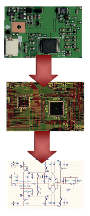
ScanFAB is a fully integrated, stand-alone, scanner based re-engineering system that permits the creation of CAD data (DXF/Gerber/Drill/CNC) from existing multi layer PCBs, parts, photo tools, stencils, drawings, microfiche, PDF files, X-Ray images, etc.
It also contains a full Gerber editor that can be used to import, modify and export Gerber & Drill data.
Uses Windows-based software linked to a high-resolution, calibrated flatbed scanner. This combination allows for accurate reverse engineering and precise reproduction of data to exact form, fit and function for today’s high density PCB board designs, complex parts and tooling.
✔ Necessity: Create high quality CAD data for legacy
products that is required for PCB
fabrication, test and repair.
✔ Accuracy: Extracted data is exact Form, Fit and
Function, eliminating need to re-certify &
retest for compliance (UL, CE, etc.)
✔ Accuracy: Eliminate errors caused by old hand
digitizing, hand-taping or camera step
and repeat methods.
✔ Accuracy: Increase board quality by using internal
check features.
✔ Security: Prevent film/drawing deterioration by
storing images in electronic format.
Product Functions
insert_emoticonSimple Process Flow
The process of image capture in B&W, Gray or Color through the conversion of raster to vector data followed by several quality control steps and finally the output in a wide variety of formats is all done in a logical, intuitive and well designed platform. Support materials include context sensitive help and work flows with embedded training videos, etc.
brightness_autoAutomatic Features
Offers various functions to quickly and automatically “vectorize” the scanned image:
• Flash Pads (circular, square, oval, rectangle)
• Tracks (orthogonal/all angle)
• Silkscreen, Solder mask
• Copper Fill Areas/Ground & Power Planes
• Crosshatched Areas (90°/45°)
• Stencil Files
• Pads and tracks on grid
• Step & Repeat
• Drill & Route CNC data
verified_userVerification
Use ScanFAB's "check functions" to verify the quality and accuracy of the data:
• Verify layer-to-layer pad alignment
• Check Gerber image vs scanned image
• Check Gerber image vs another Gerber image
• Compare one scanned image to another
• Design rule check
• Highlight D Codes
• Delete "double-hit" pads
• Verify track & pad connections
• Check for potential shorts & opens
printScanning
• Flex, Ceramic & FR4 substrates, film, paper, stencils, screens, diazo, silver, glass & chrome
• Single, Double & Multi-layer PCBs
• Verifiable image alignment & deskew
• Automatic layer-to-layer alignment
• Up to 99 layers in each job
Product Features

Output Files
• Gerber files (274X or 274D)
• Comprehensive aperture tables
• Drill files: Excellon, Sieb & Meyer
• Stencil files
• Soldermask, Padmaster, Silkscreen
• Circuit, Ground/Powerplane
• DXF
• BMP, TIFF
• Panelized images

Output Files (Optional)
• ODB++
• FATF
• IPC-D 356
• EDIF version 2.0
• Orcad PCB II wirelist
• Scicards netlist
• Specctra & Maxroute autorouters
• EED3 layout wirelist
• CUPL netlist
• XILINX netlist
• JEDEC netlist
• ALTERA netlist
• Export CNC data in G-CODE
• EDWinXP schematic netlist
• DXF

Other Modules (Optional)
• Extract component information including
component centroid, rotation, part number,
package ID and reference designator.
• Generate package footprint, pin numbering &
netlist information with industry standard
outputs that can be imported into most CAD
packages.
• Component centroid data (70+ machines)
• Create component vision library files
• Netlist generation
• Automatic Pin Numbering
• Generate Schematic & PCB layout
• 28,000+ Part Library
• Many CAD interfaces
• SPICE based simulator and thermal analyzer
• Electromagnetic Analyzer (with Signal
Integrity and Field analyzer)
Want to know more?